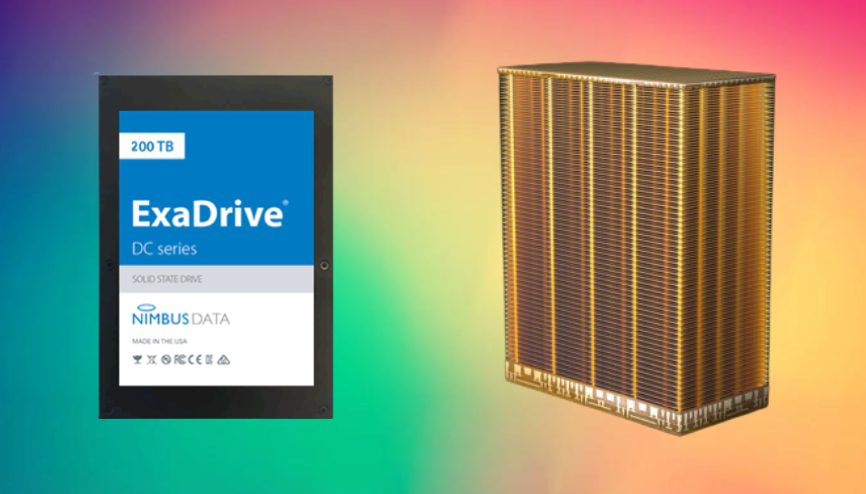
As the technology is updated day by day, there is a lot of emphasis on faster and faster Nvme, which is barely noticeable, while the actual capacity is stagnant at around 2-4Tb. As someone very interested in photography, it doesn’t take too long to fill up 2Tb of space. It’s the first time a NAND maker has broken 200 layers, and the previous flagship chip, a 176-layer model last announced in November 2020, has improved by nearly 32% (or 56 more layers) in less than two years. The company says it will enable faster data up to transfers of more than 50% than the design of 176-layer. Having increased write bandwidth chance to achieve 100% and 75% more read bandwidth.
Companies that make their NAND and ASICs have a high level of understanding of how all the parts of an SSD integrate into a single product. They can push the boundaries of how NAND and ASIC interact, squeezing every bit of performance out of individual components. Over the past few months, we’ve seen innovation taking place on two fronts: ASIC design and NAND technology. Each area presents highly complex issues that have in some cases been relatively ignored.
Other reference values for the number of layers were 64, 96, and 128 products. Rumors suggest that the new chip is physically smaller than the previous generation and has the highest areal density of any silicon-based data storage component. This means that the new technology will support the launch of even smaller products and enable those with larger capacities, including SSDs and microSD cards.
According to Micron the move to layers at 232 allows for a 35 to 100% increase in density when compared to competing for TLC designs. Micron did not confirm what manufacturing technology was used to etch the TLC chip but added that the chip has the highest I/O speed in the entire market at 2.4 GB/s, which is 50% faster than the previous generation. Micron may also have plans to launch high-density QLC plans; this may help narrow the cost-per-capacity gap even further for hard drives, bringing them even closer to obsolescence, at least in data centers.
Another innovation that Micron brought is the use of NV-LPDDR4 memory, which greatly reduces the power consumption needed to transfer bits, reducing it by almost a third, which will help reduce the overall power consumption of the system and can improve battery life. The small package naturally allows for a “diverse deployment set” along with cellular, edge, and many others. Micron may also pioneer the use of NV-LPDDR4 reminiscence. This low-power response reduces the amount of power required for propulsion by roughly 30%. The company said it is currently shipping 232-layer NAND from its Singapore factory. It delivers it in element type and through its important SSD product line.


